
metalworkingmag.com
22
'26
Written on Modified on
Chemical Etching Bridges Prototyping and Volume Metal Production
Precision Micro explains how photochemical etching uses one low-cost tool from first samples to high-volume runs, reducing revalidation and tooling costs.
www.precisionmicro.com
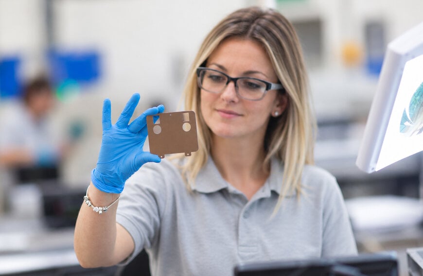
Scaling a validated prototype into volume manufacturing is a recurring bottleneck for producers of precision metal components in electronics, semiconductor and automotive applications. Precision Micro, a UK-based chemical etching specialist, sets out how photochemical etching can keep the same tooling and process from first samples through to high-volume production.
Why the prototype-to-production transition is costly
According to Protolabs' Innovation in Manufacturing 2026 report, 97 per cent of companies report delays or failures when bringing products to market, with scaling to production identified as the biggest challenge for product developers. Electronics and semiconductor products often have short development cycles, so any tooling change and revalidation between prototype and series production directly affects time to market.
In stamping and pressing, prototypes are often produced with soft tooling made from steel that is easier and cheaper to machine. Such tools typically last between 10 and 10,000 cycles, compared with around one million cycles for hardened production tooling. Once the design is validated, hardened tooling must be built and the component validated again with the new tool and process. With production tooling potentially costing five or six figures, this step becomes a significant hurdle on the way to volume manufacturing.
The issue is gaining relevance as investment in product development rises. The European Investment Bank's 2025 Investment Survey found that 32 per cent of EU firms engage in innovation, compared with 53 per cent in the US, while the 2026 Make UK and PwC Executive Survey reports that 68 per cent of UK manufacturers are increasing investment in new product development.
How photochemical etching scales across production volumes
Chemical etching removes metal selectively through a photo-defined mask rather than by mechanical cutting. According to Precision Micro, development tooling costs around £100, and the same tooling and process can support production of 100 samples or 100,000 components. Output can therefore scale without automatically requiring new tooling, although testing and validation are still needed to confirm that components meet the required specifications.
Low tooling costs also make design iteration more economical. A filtration mesh, for example, can incorporate six variations of hole size and spacing on a single sheet using one tool, where the design allows, with samples delivered in seven days.
Material thickness, properties and design complexity
Chemical etching is typically used for metal thicknesses of up to around 1.5 mm, although materials up to 2.5 mm thick can be processed. Within this range, engineers can trial different material gauges without the tooling modifications that stamping may require, where a change in thickness affects clearances and radii and can cost thousands of pounds and take weeks.
The process handles both soft and hard metals, including specialist stainless steels used for springs. Because it does not apply the mechanical forces of stamping or create the heat-affected zones associated with laser cutting, it preserves material properties and avoids stamping-related burrs. Cleaning is also incorporated into the process.
Etching can produce numerous holes and intricate channels simultaneously, which suits parts ranging from flow channels in semiconductor cooling plates to automotive speaker grilles.
Etched components in automotive and safety-critical production
In automotive applications, Precision Micro developed etched springs that became a standard component in fuel pumps, ABS braking systems and catalytic converters. In gasoline direct injection (GDI) systems, etched components are used in high-volume, safety-critical applications where manufacturing consistency is essential and 100 per cent inspection is carried out across more than 1,000,000 components per month.
According to Ben Kitson, head of business development at Precision Micro, considering production volumes, material requirements and performance specifications early helps avoid expensive changes later, while working with a supplier equipped for both development and high-volume manufacturing maintains continuity as requirements evolve.
Additional Context
This section details technical specifications and competitive benchmarking not included in the original product announcement.
Photochemical etching, also known as photochemical machining, transfers the part geometry from a phototool onto metal coated with a UV-sensitive photoresist. After exposure and development, a heated etchant, typically ferric chloride, dissolves the unprotected metal from both sides. Precision Micro's published design guidance specifies a minimum standard tolerance of ±0.025 mm for thicknesses from 0.01 to 0.25 mm, typically ±10 per cent of material thickness up to 2.5 mm, and a standard minimum feature size of 0.1 mm.
By comparison, laser cutting is a single-point thermal process that the same guidance associates with tolerances of around ±5 per cent of thickness and a typical minimum feature size of 0.2 mm, with costs rising for parts with many openings. Stamping offers low unit costs at high volumes but relies on dies costing thousands, with lead times of six to eight weeks, while wire EDM is limited to conductive metals and involves high equipment costs. Process selection therefore depends on part geometry, thickness, volume and edge-quality requirements.
Edited by Sucithra Mani, Induportals editor – adapted by AI.
www.precisionmicro.com
